|
Shenzhen XingdaYun Technology Co., Ltd.
|
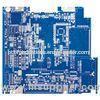
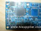
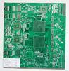
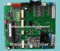
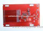
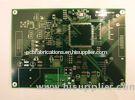
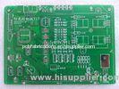
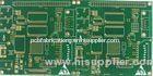
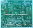
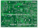
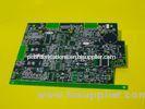
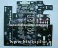
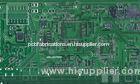
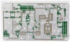
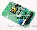
UL & ROHS high standard Double Layer HASL Lead Free PCB for LED circuit board
| Place of Origin: | Zhejiang, China (Mainland) |
|
|
|
| Add to My Favorites | |
| HiSupplier Escrow |
Product Detail
UL & RO
UL & ROHS high standard Double Layer HASL Lead Free PCB for LED circuit board
Specifications
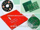
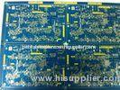
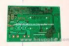
2.2 Layer white solder mask pcb
3.UL&ROHS approved LED pcb
4.Small order is accptable
Detailed Product Description
1.Shenzhen high standard LED pcb
2.Double layer white solder mask LED pcb
3.High quality HASL lead free LED pcb
4.ICT function and testing instruction test
5.many years OEM,ODM,IC program&test
6.Competitive price and quick delivery
Layer: 2 Layer
Material: FR4
Thickness: 1.6mm
Copper thickness: 1oz
Mini Hole: 0.2mm
Mini Width/space: 0.1mm/0.1mm
Testing points:4000
Solder Mask: LPI White
Sickscreen: Black
Function: LED
Finish: HASL lead free
PCB Manufacture Capability
|
Item |
Capability |
|
|
1.Base Material |
FR-4 / High TG FR-4 / Lead free Materials (ROHS Compliant) / Halogen Free material /CEM-3/CEM-1/ /PTFE/ROGERS/ARLON/TACONIC |
|
|
2.Layers |
1-28 |
|
|
3.Finised inner/outer copper thickness |
1-6OZ |
|
|
4.Finished board thickness |
0.2-7.0mm |
|
|
Tolerance |
Board thickness≤1.0mm: +/-0.1mm 1<Board thickness≤2.0mm: +/-10% Board thickness>2.0mm: +/-8% |
|
|
5.Max panel size |
≤2sidesPCB: 600*1500mm Multilayer PCB: 500*1200mm |
|
|
6.Min conductor line width/spacing |
Inner layers: ≥3/3mil Outer layers: ≥3.5/3.5mil |
|
|
7.Min hole size |
Mechanical hole: 0.15mm Laser hole: 0.1mm |
|
|
Drilling precision: first drilling |
First drilling: 1mil Second drilling: 4mil |
|
|
8.Warpage |
Board thickness≤0.79mm: β≤1.0% 0.80≤Board thickness≤2.4mm: β≤0.7% Board thickness≥2.5mm: β≤0.5% |
|
|
9.Controlled Impedance |
+/-5% |
|
|
10. Aspect Ratio |
15:1 |
|
|
11.Min welding ring |
||